|
About Us
Contact
S.S.PCB
D.S.PCB
MULTI PCB
HDI PCB
Aluminum Based-PCB
FULL FLEX PCB
Major Client
Technics Flow Line
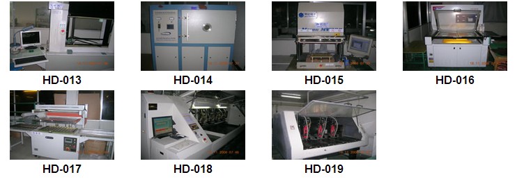
Major Equipment
100 top world PCB makers
Certificate
News
Trademark and its Brand
PCB Quote
Service1: Overseas Overseas
Service2:Overseas
Service3:Domestic |
|
Welcome to huading-group
Double Side board Main Application:
Consumer、Telecom、Industrial、Aero Industry

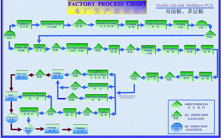
Technical Flow Chart
Plant

Technological Advantages
|
Processing capabilities in many fields:
● Double-sided ~ High Multi-layer PCB (max. 40-layer)
● HDI (2+X+2 Build UP)
● HDI thin PCB (0.25mm for 4-layer, 0.40mm for
6-layer)
● Big size, Back plane PCB (Panel size at
24”x36”, Thickness of 4.5mm or more)
● Special-purpose PCB (Heavy copper(6oz) PCB, /
Buried resistance PCB)
● Via hole copper plating
● Thick gold
● Uneven gold finger |
|
Workstation |
Content |
|
Inner layer imaging |
Both wet and dry film, auto-exposure
machines from Japan, horizontal etching
lines from Germany, enhancing the capability
to produce min. 40μm -thick CCL and min.
width/gap 40μm/40μm. |
|
Laminating |
Leading integrated hot and cold laminating
machines from Germany, able to process up to
40-layer PCB. Pressing the min. thickness of
0.20mm, the max. thickness of 5mm or more,
with excellent thickness uniformity. |
|
Mechanical drilling |
HITACHI CNC drilling machines to ensure the
min. hole diameter of 0.10mm with high
precision. |
|
Laser drilling |
HITACHI CNC laser drilling machines to
ensure the min. hole diameter 0.075mm,
drilling speed 20,000 holes / min or more,
high-density interconnect board producing. |
|
Copper plating |
Pulse plating / Continuous vertical panel
plating, special tools for 40μm -thick CCL
,to achieve Aspect Ratio with 20:1 and good
copper distribution COV≤6%. |
|
Copper electroplating micro via filling |
Applying selected special chemical additives
,optimized ?electroplating process parameter
,together with the appropriate
electroplating equipment, to ?fulfill the
high-end customer's requirement on high
quality of high board thickness to via
diameter ratio blind via and through via
filling capability, to ensure the
reliability of the HDI PCB. |
|
Solder mask print |
E-spray technology, able to print over 0.1mm
thin PCB, and max.12 oz heavy copper with
solder mask thickness≥5um on trace edge. |
|
Electrical Test |
Four-terminal tester, the min. test pad
diameter at 0.1mm, min. test resistance at
10 milliohms to ensure quality and
reliability of the HDI PCB. |
|
Special carbon printing |
Special configuration of the carbon &
dielectric paste print line, life test up to
18 million cycles to ensure product
reliabilities. |
|
|
|
|
|