ʲô�����壿
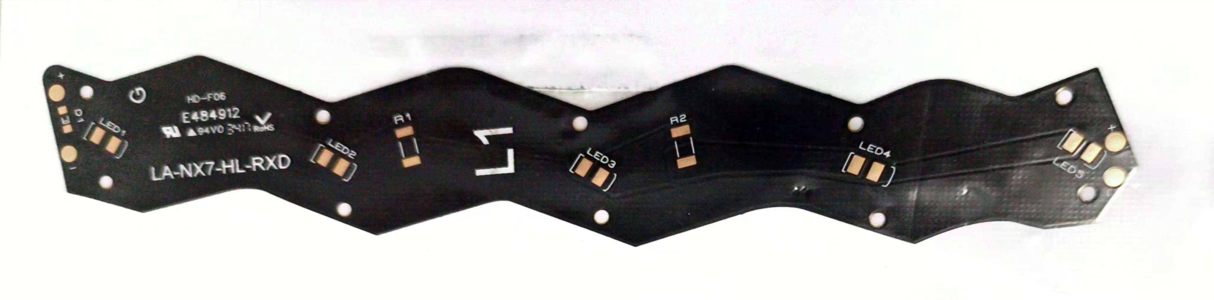
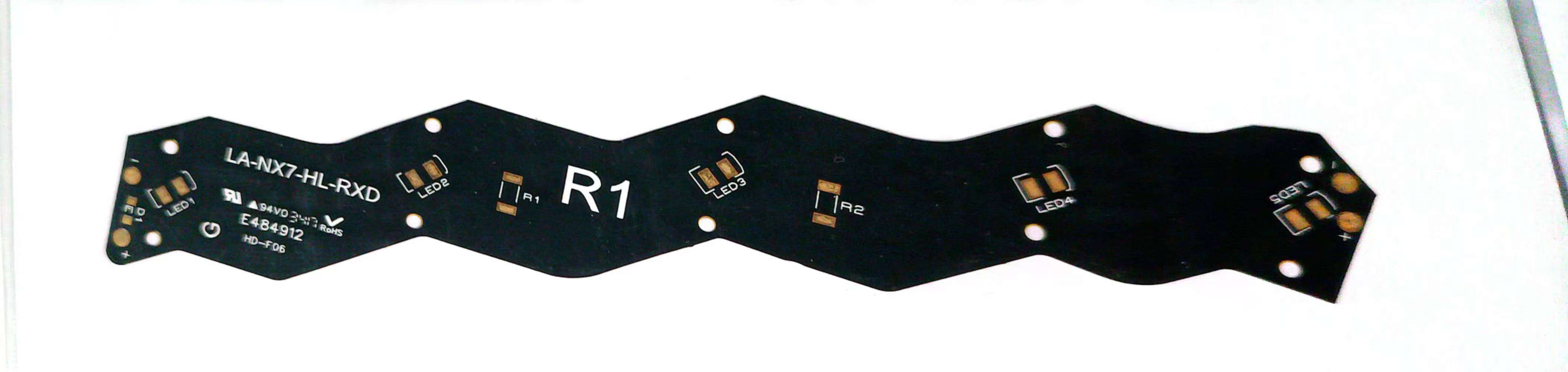
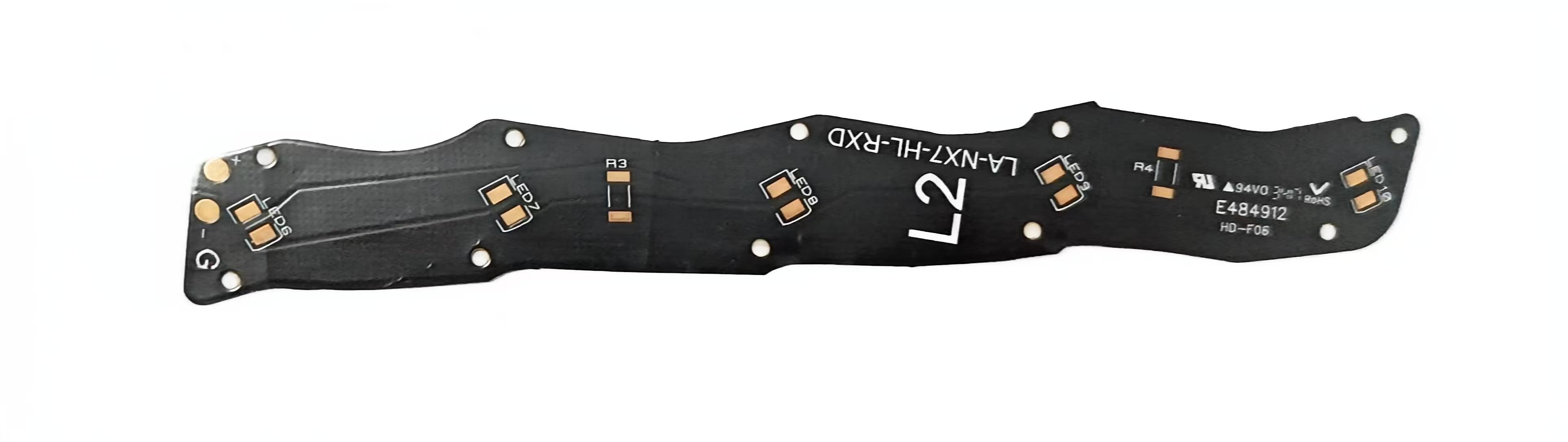
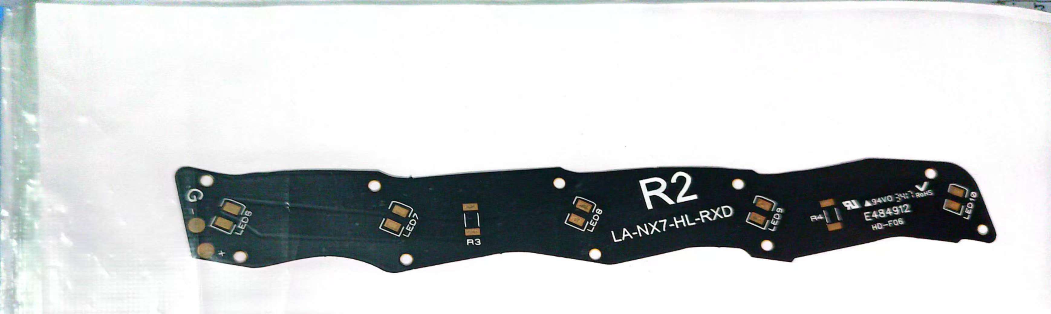
���壨FPC���������Ծ�Ե����Ϊ���ģ������ۡ����۵���ӡ�Ƶ�·�壬�㷺���ڿռ����Ͷ�̬Ӧ�ó�����
������ص�
���������
��������������ԣ�������ά�ռ������������۵�����Ӧ���ӽṹ��ơ�
��������
��ȿ�����0.1mm���£��������ᣬΪ�����͵��Ӳ�Ʒ�ṩ������������
��̬�ɿ���
��������ƿɳ�������������۶���ʧЧ���ʺ϶�̬����Ӧ�ó�����
���ɻ����
�����ͳ���º�����������ϵͳ�ṹ���������ӿɿ��Ժ��ȶ��ԡ�
������Ҫ����
�����ǰ���PI��
��ͭ����RA��
��ͭ����ED Copper��
�߿ɿ��Խ�ϵ
������
�ṹ����
��������
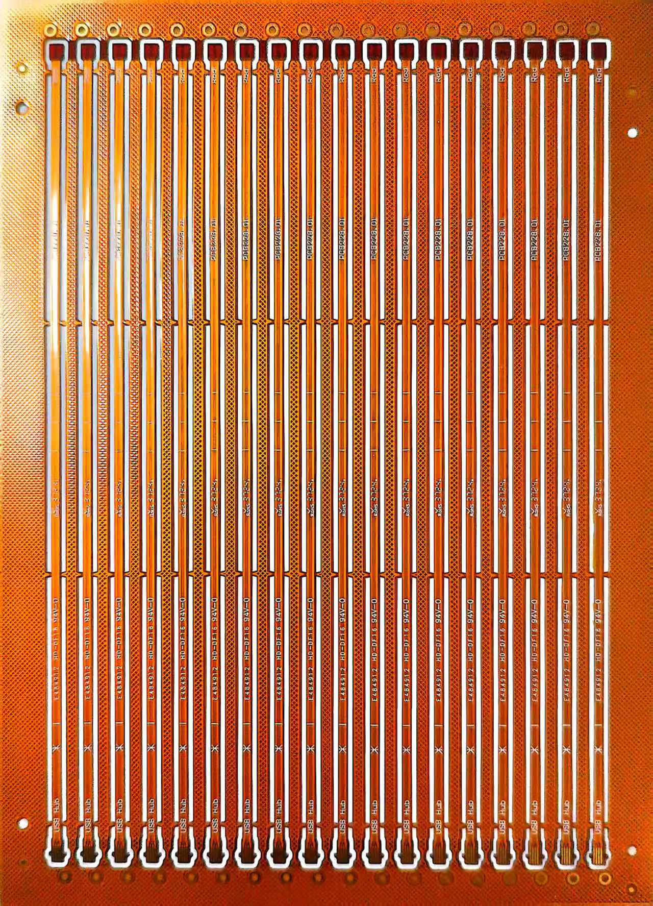
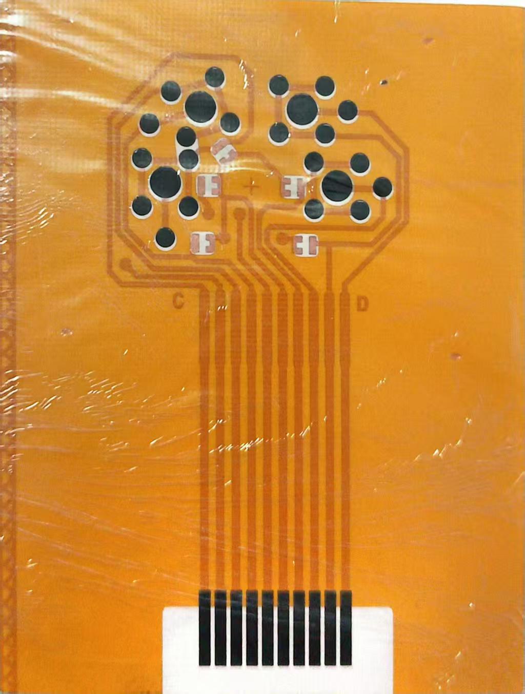
Basic Flexible PCB
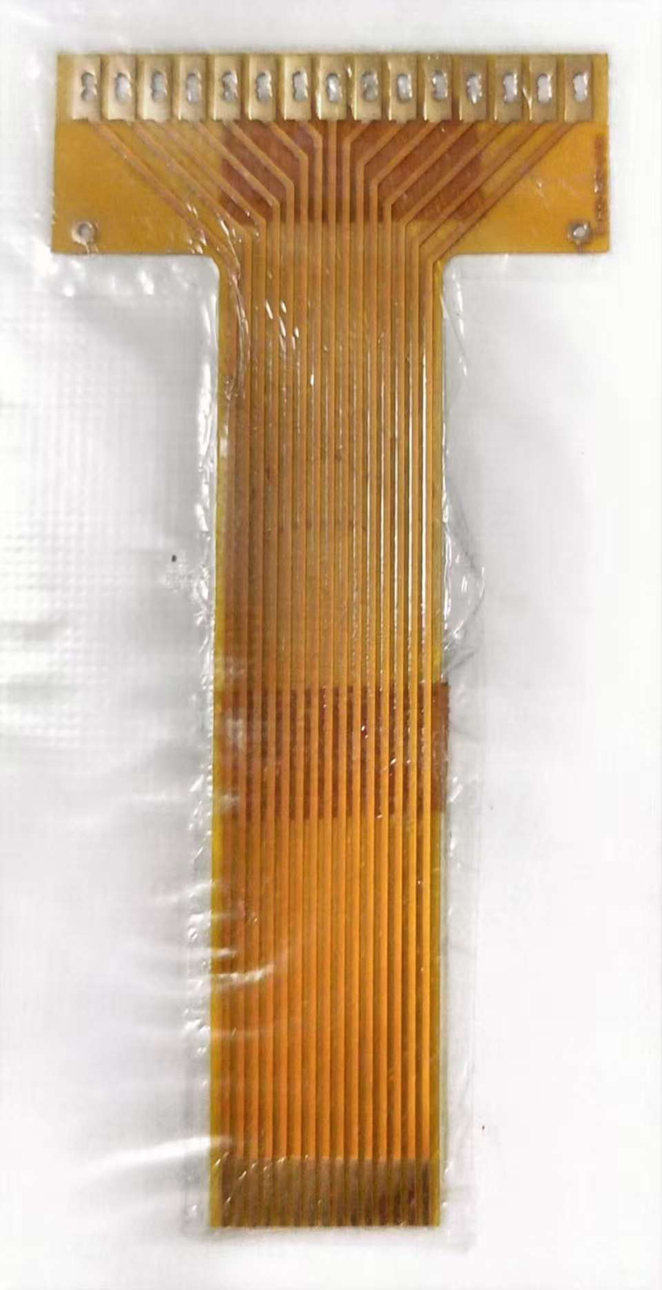
˫������
Double-sided FPC
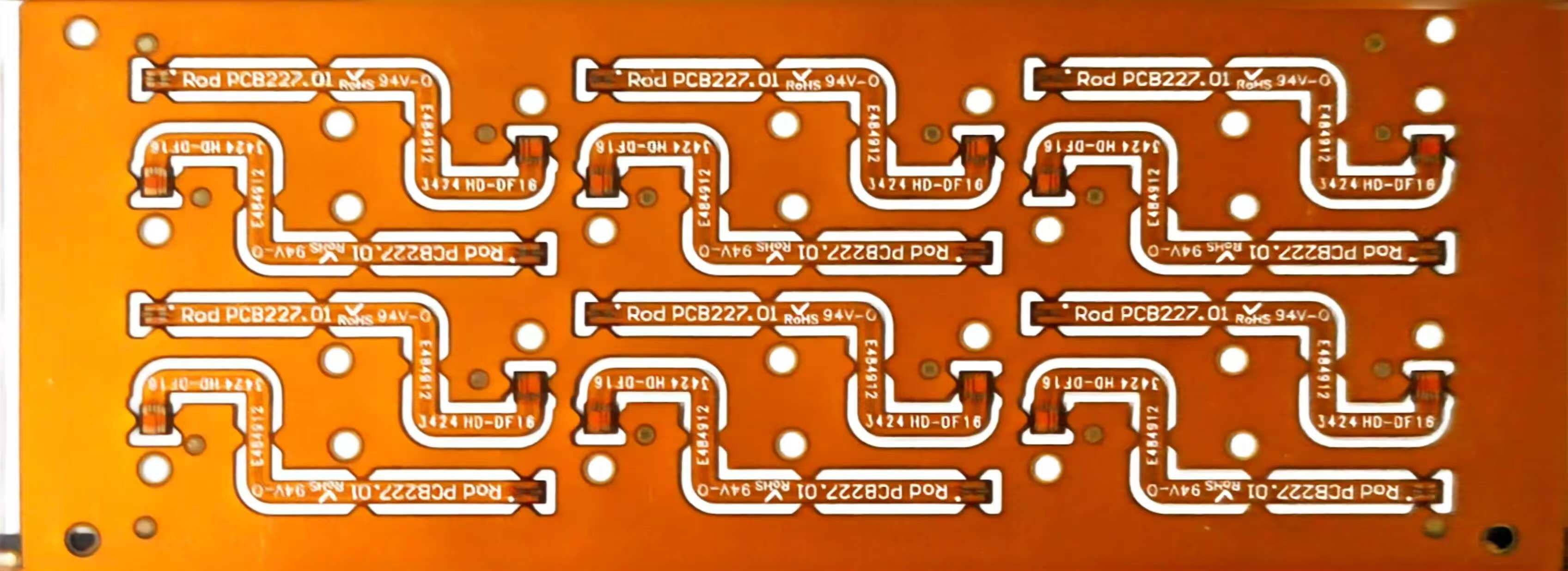
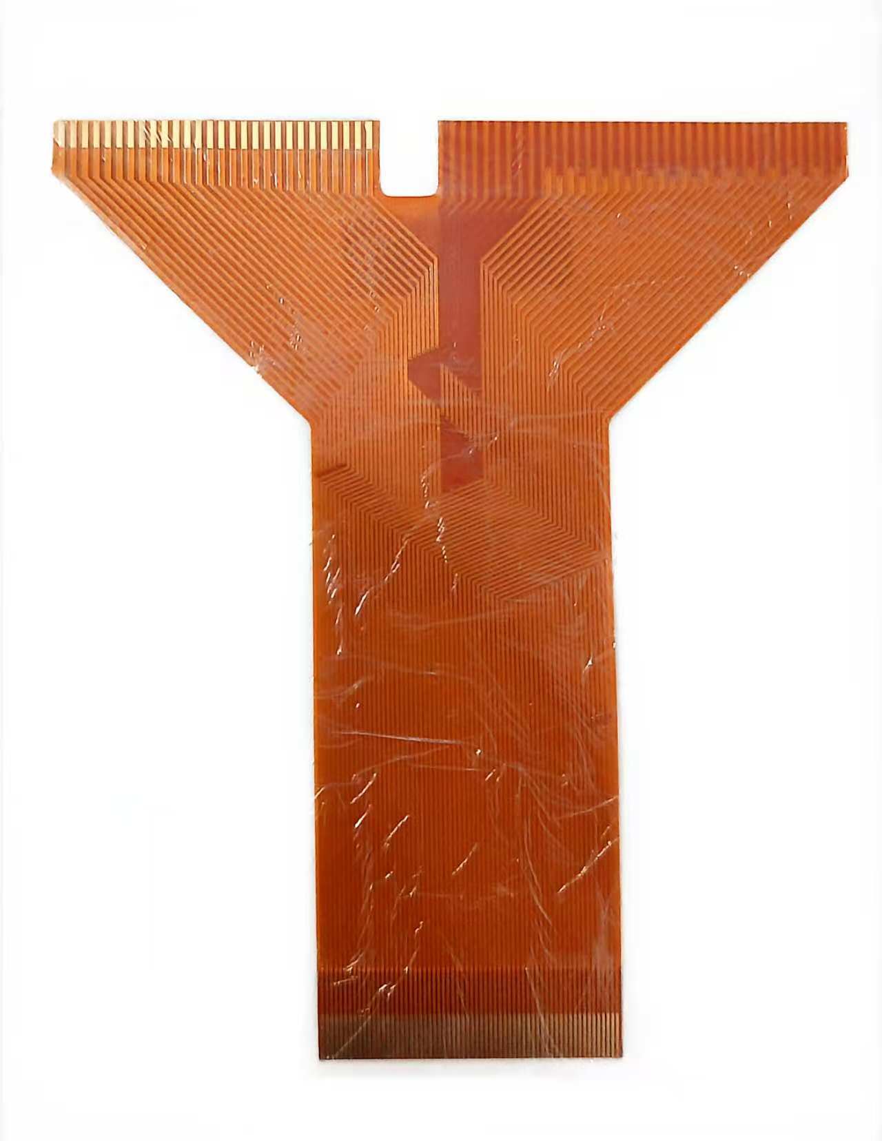
�������
Multilayer FPC
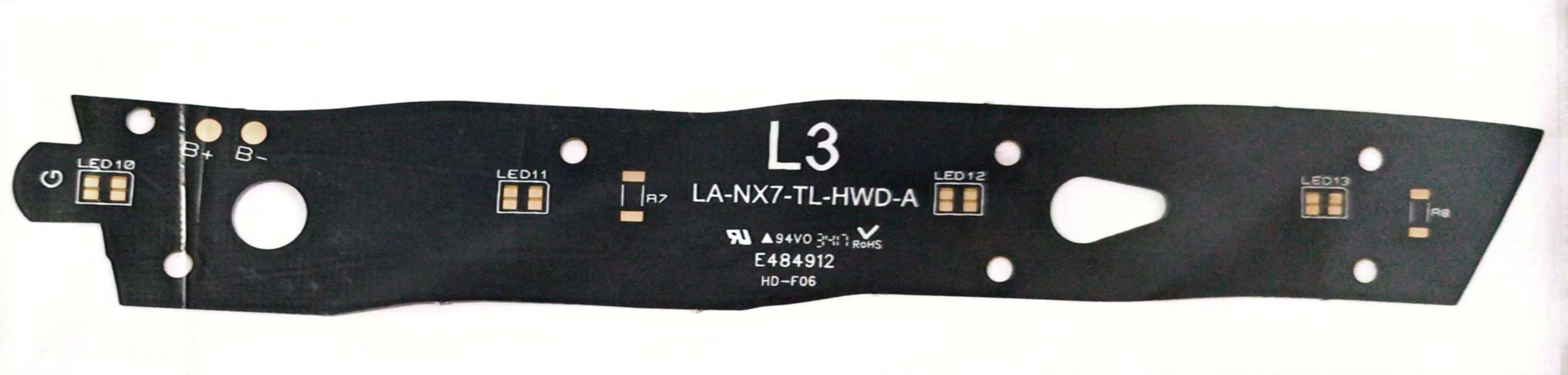
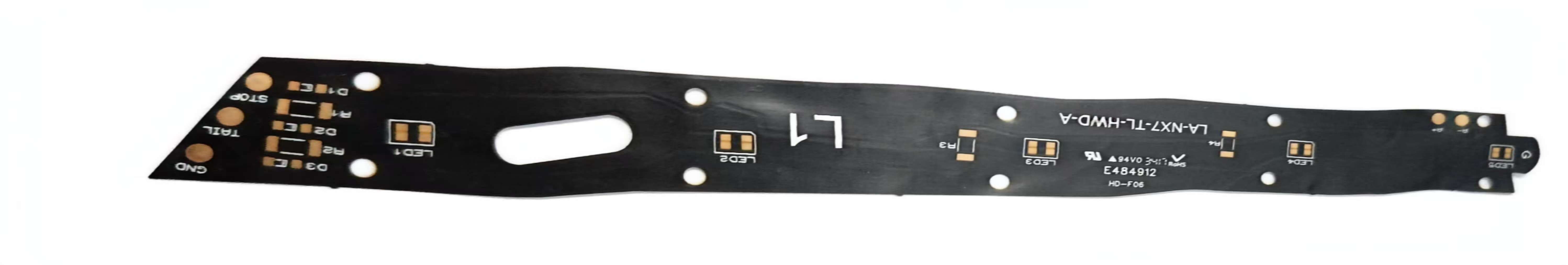
�����ϰ�
Rigid-Flex PCB
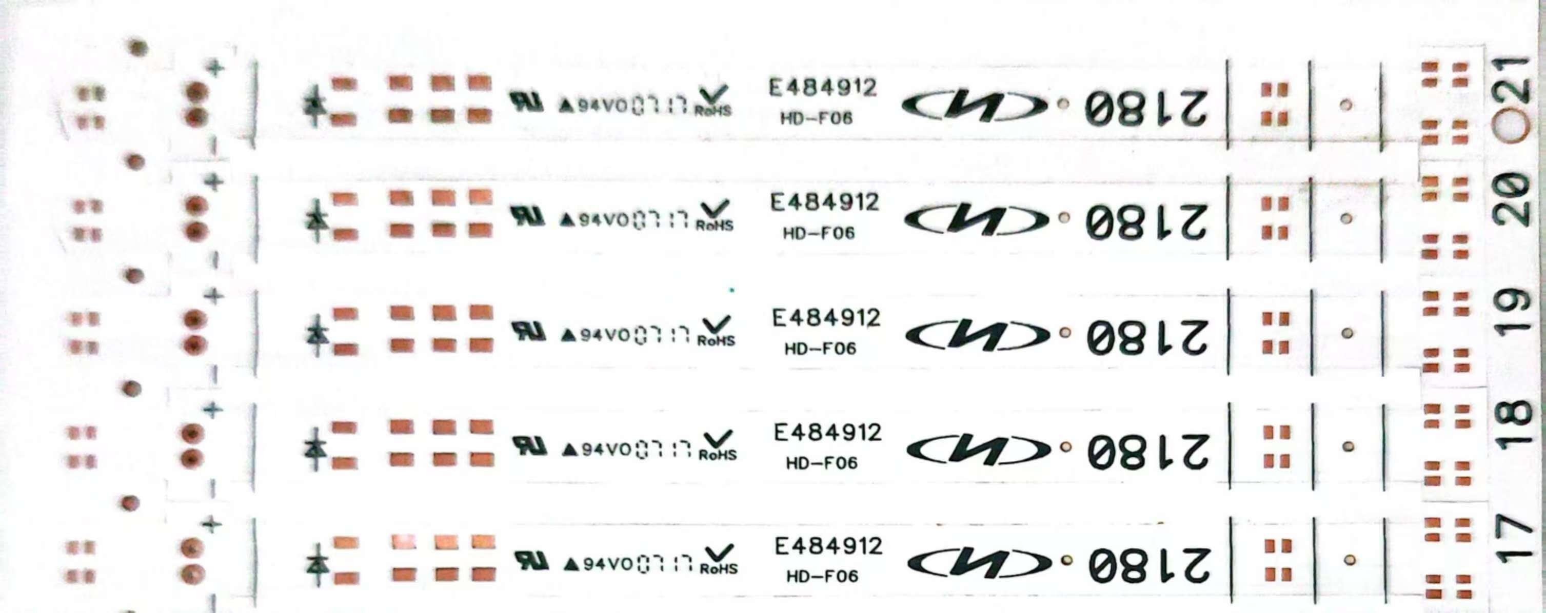
�7�7 ���������ϵ�����ṩ UL ��֤֧�֡�
����Ӧ�ó���
���ѵ���
ҽ���豸
��������
��ҵ�豸
��������ʾģ��