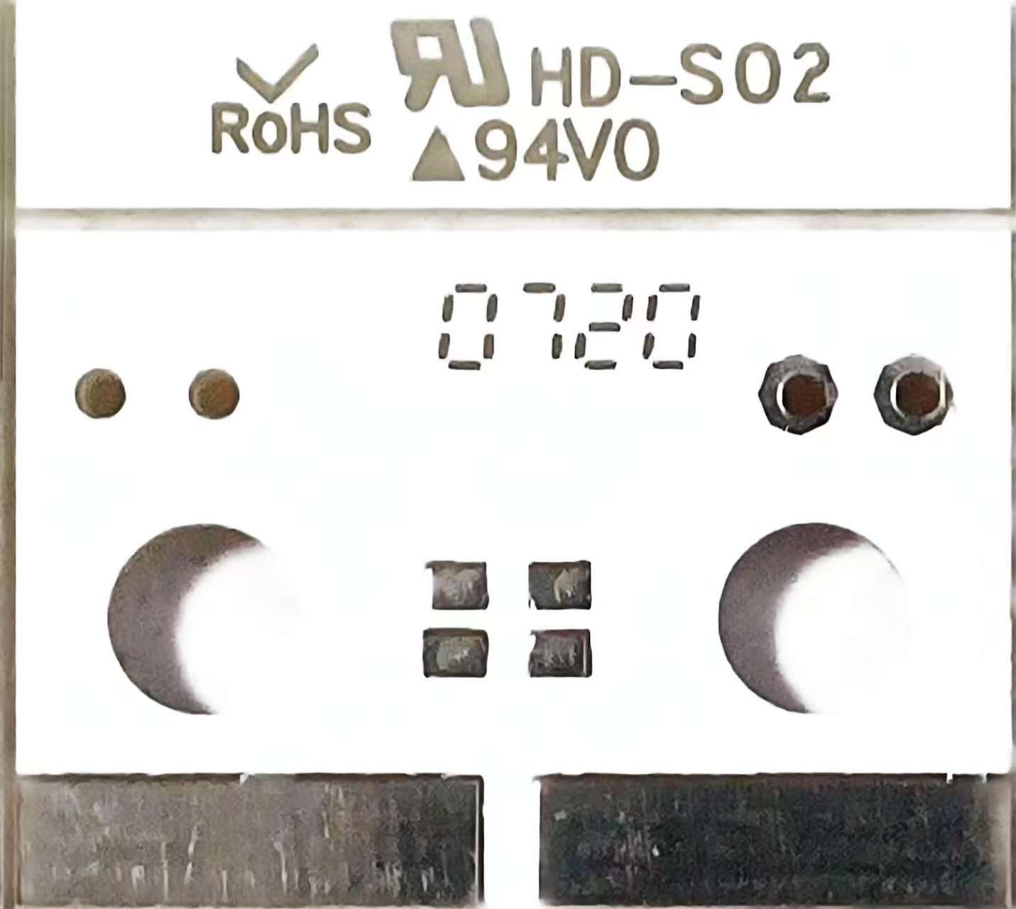
ʲô�ǵ���壿
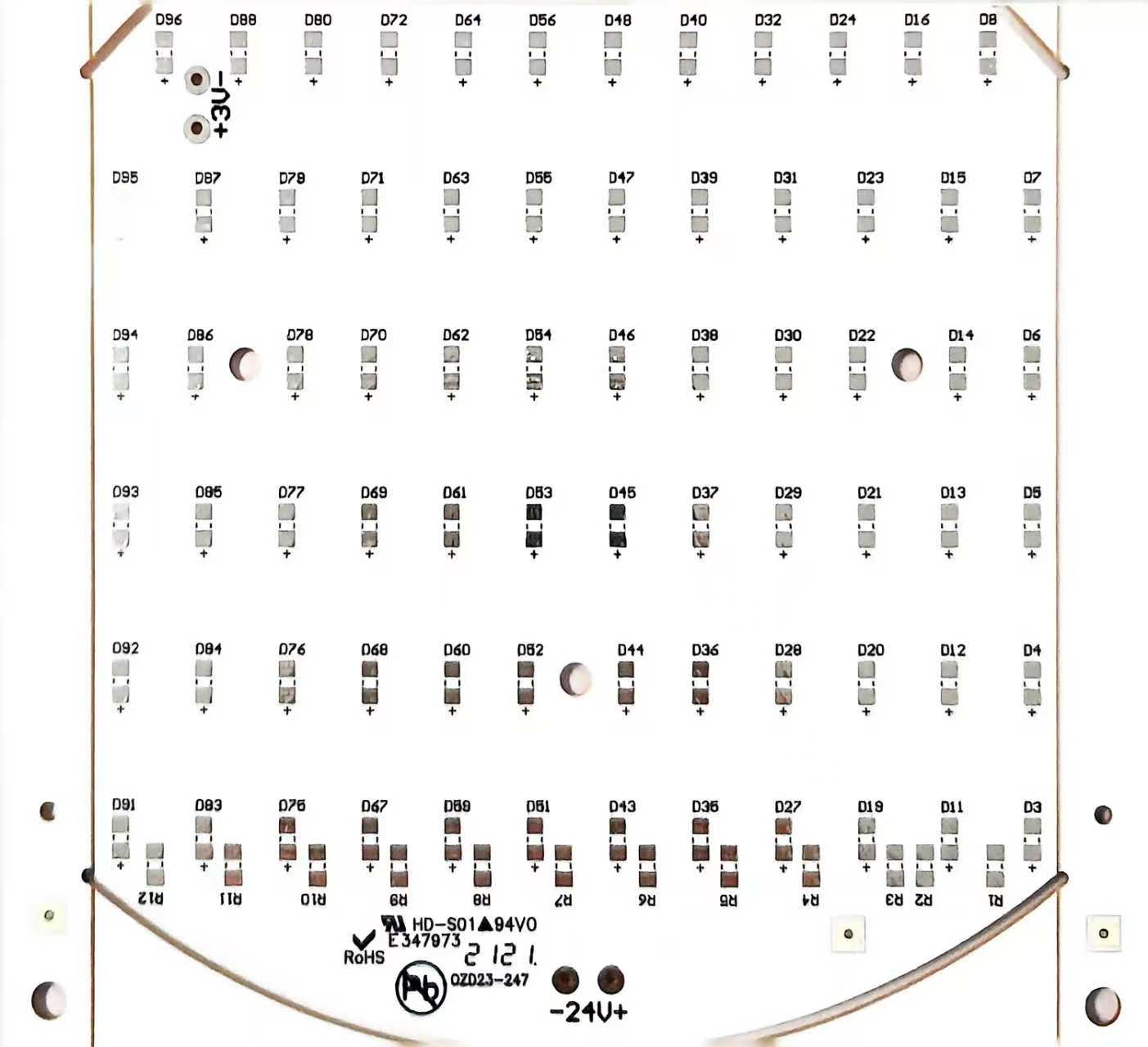
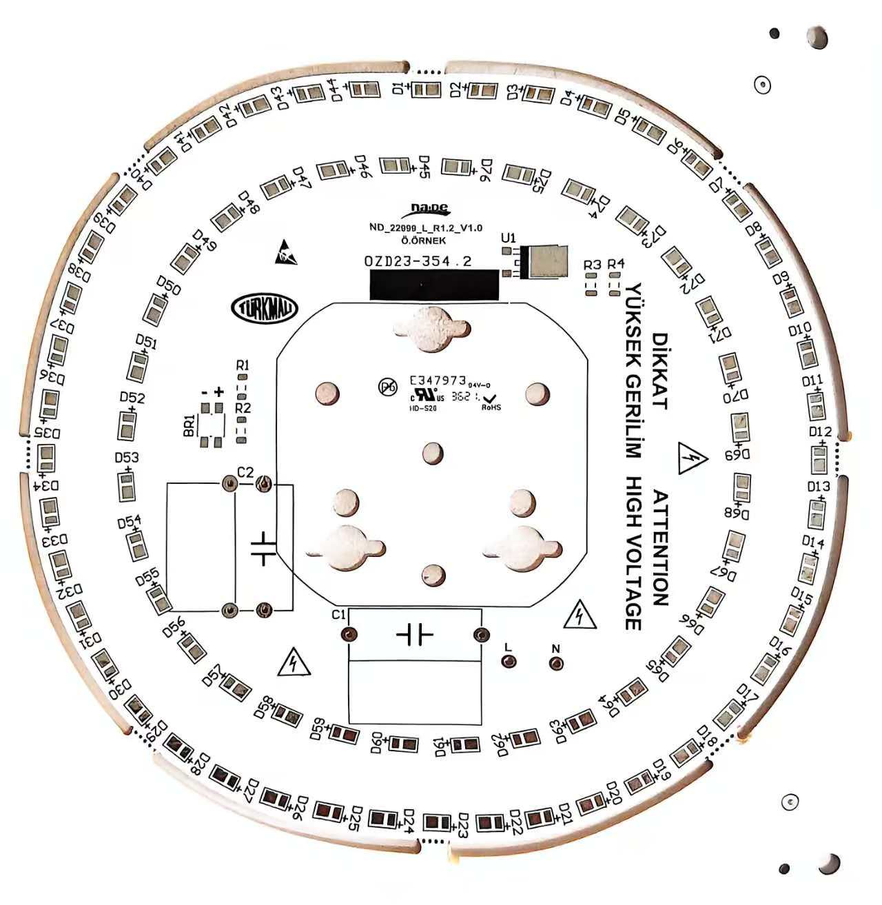
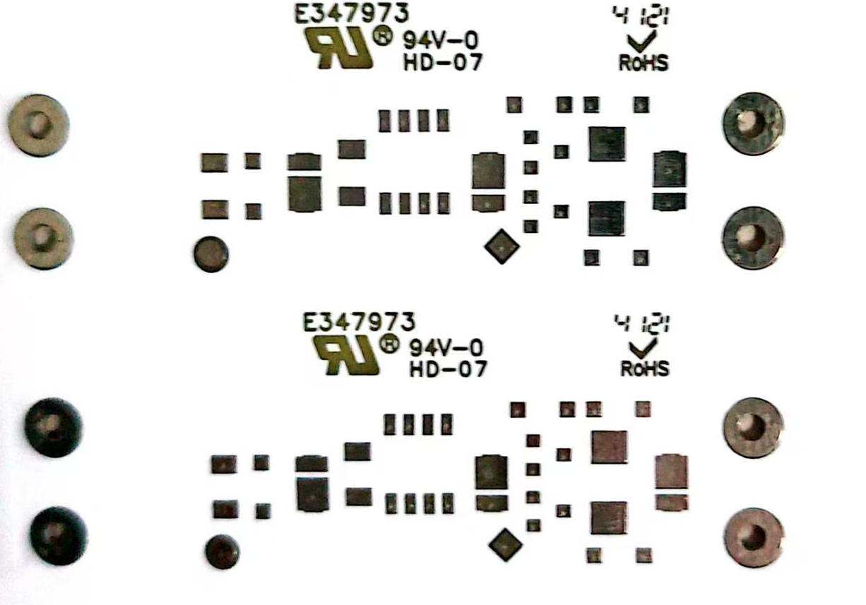
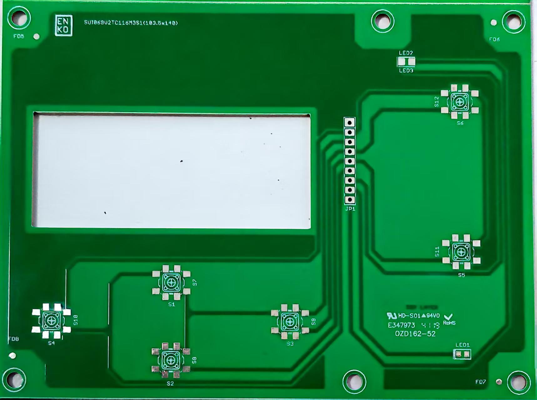
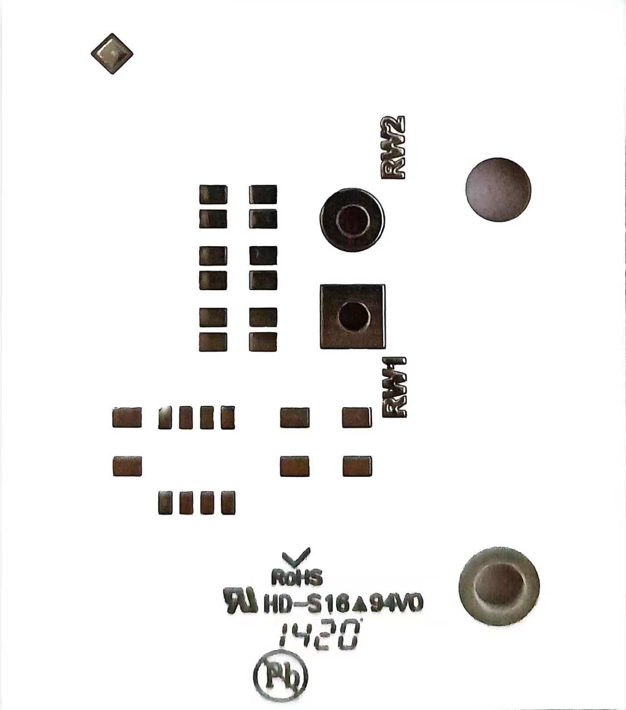
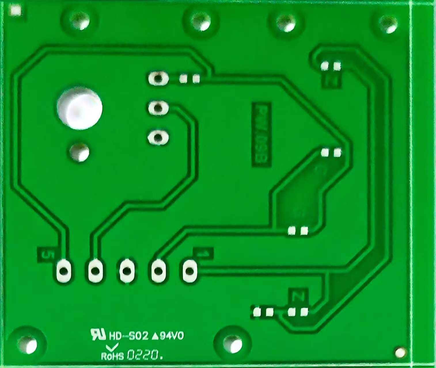
�������ָ���ڻ���һ�าͭ���γ���·��ӡ�Ƶ�·�壬���������Ӧ����㷺��һ�� PCB��
�������ص�
�ṹ��
���㲼����ƣ����칤�ճ����ȶ��������������ڿ��ƣ����ʸߡ�
�ɱ�Ч���
���������٣��������̼������ɱ��ͣ��ر��ʺϴ���������Ӧ�á�
�ɿ��Ը�
���ӵ�һĿ��Ȼ��ά�ͼ�ⷽ���ݣ���Ʒʹ�����������ɿ��Ըߡ�
���������ǿ
�����ڵ��ܶȡ����Ӷȵ�·��ƣ������ż����Ӳ�Ʒ�����ѡ��
����峣�ò���
XPC
FR-1
FR-2
FR-3
FR-4
CEM-1
CEM-3
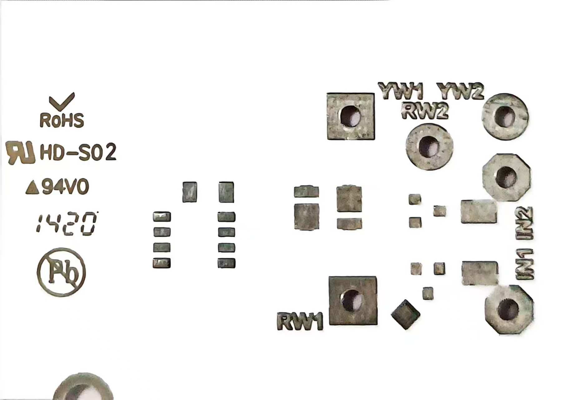
������֤��Ϣ
��������
ֽ��/����������
��ȼ�ȼ�
UL94 V-0/V-1/V-2
��ȷ�Χ
0.8mm - 3.2mm
�7�7 �������������ȫϵ�е������ϵ� UL ��֤�������㲻ͬ�г�������Ҫ��
������Ӧ�ó���
��������Ӳ�Ʒ
������ܱ��豸
ͨ���ն��豸
���õ������ư�
��ҵ��������ģ��